Beyond Pass/Fail: Characterizing Silicon Margin With PVTW
Determining not only whether a device meets specification, but how far it is from the boundary, helps inform product robustness and future design decisions.
Recent stories from Semiconductor Engineering.
Determining not only whether a device meets specification, but how far it is from the boundary, helps inform product robustness and future design decisions.
Moving voltage regulators closer to processors can reduce power loss, but adds challenges for advanced packaging, thermal management, and system-level design.
Model process variation, detect multiple failure modes, and evaluate solutions with less wafer experimentation.
Operationalizing intelligence across the manufacturing stack begins with trusted data.
The high number of new and upcoming production lines is a unique factor influencing this particular cycle.
Linking plasma chamber simulation with feature-scale process modeling to predict etch profiles, evaluate wafer uniformity, and optimize plasma etching processes.
Multiple designs are emerging for CPO and NPO, but standardization and high-volume manufacturing are still not ready.
AI can optimize processes and find defects, but autonomous decisions require better data and strict process controls.
Agentic AI promises to automate more of the chip flow, but integration with EDA tools and capturing decades of engineering expertise are non-trivial.
PCIe and trust; rack-scale co-design; heterogeneous scaling; AI data center primer; on-device balancing; EU semi trends.
Researchers at Arizona State University and Ampere Computing published “DT-MATCH: Defect- and Topology-Aware Chiplet Matching for Yield Optimization in Heterogeneous Integration.” Abstract “Heterogeneous integration (HI) and advanced packaging enable chiplet-based system-on-chip (SoC) designs; however, they also introduce new yield challenges arising from manufacturing defects and complex die-to-die (D2D) interconnect constraints. In particular, lane-level defects…
Researchers at Korea Advanced Institute of Science and Technology (KAIST) published “Clock Distribution Network with Backside Clock Mesh in BSPDN Architecture.” Abstract Excerpt “We propose a clock distribution network (CDN) in which the clock mesh is located on backside metal (BM) layers, while the rest of the network remains on the frontside. Since the backside... »
Why both approaches are needed at angstrom-level dimensions.
HBM4 controller partitioning; single-crystal high-κ dielectrics for low-power 2D CFETs; HW-based location checks for AI chip smuggling; embedded ECC for AI weight protection; optimized e-beam evaporation for metal-semiconductor contacts; sub-volt HZO ferroelectric capacitors; randomized-cache HW security.
Researchers at Singapore University of Technology and Design (SUTD), A*STAR, and National University of Singapore (NUS) published “Self-Supervised Attention-Based Virtual Metrology for CMP MRR Prediction.” Excerpt “In this paper, we propose Global Regression Pretraining (GREP), a self-supervised, attention-based framework for CMP* MRR prediction. GREP learns temporal representations from unlabeled sensor signals through global proxy-target regression,... »
Researchers at Georgia Tech, NVIDIA Research, and Stanford University published “SlipStream: Enabling HBF for GPU Systems by Mitigating the Latency and SRAM Overheads.” Abstract Excerpt “Large language model (LLM) inference demands ever more memory capacity for larger models and batch sizes. High-Bandwidth Flash (HBF) replaces the DRAM dies of HBM with NAND flash and provides... »
Obtaining clear images of gaps and delaminations in advanced packages.
Agents are emerging as reusable design tools, but trust and use models remain challenging.
Tharunya Yogananda and Wantong Li of the University of California, Riverside published a technical paper titled “Beyond Host-Side Control: HBM Controller Partitioning Across Host and HBM Base Dies.” Abstract Excerpt: “Recent generations of high bandwidth memory (HBM), such as HBM4, allow the base die of the memory stack to be manufactured using a logic process... »
Nvidia faces questions about security and oversight; 300mm SiC breakthrough; Siemens buys Lauterbach; chiplet standards; new memory bets; imec interposer process flow; TPUs with CPUs; 2D transistors; anti-smuggling tools for chips.
Processing data closer to memory could reduce power and boost performance, but software, thermal, and architectural challenges remain.
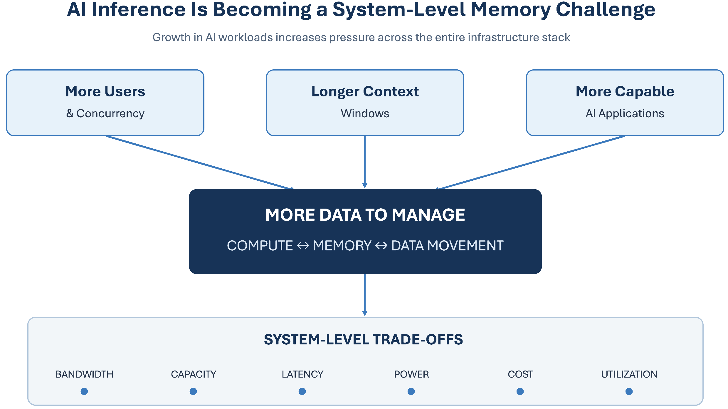
Longer contexts, higher concurrency, multimodal models, and AI agents will continue changing where memory pressure appears.
Use evidence from silicon to improve the tools and decisions that create the next generation of hardware.
Traditional voltage scaling is no longer sufficient to deliver real-time performance within tight energy and thermal limits.
Integration challenges are growing more complex, but the problem is well understood and solutions are emerging.
Right-size the memory hierarchy around the device's data streams, reuse patterns, latency requirements, and operating constraints.
The rationale behind 8-bit floating-point data formats, their ecosystem momentum, and hardware support.
Custom instructions promise flexibility, but experts question whether RISC-V belongs at the heart of AI acceleration.
How an integrated foundation IP strategy can reduce execution risk, enable faster tape-out, and lower TCO.